 |
Goddard Space
Flight Center NASA > GSFC > Astrophysics Science Division > IXO |
|

You are here: Technology» HTRS»
The High Time Resolution Spectrometer (HTRS) is proposed as a focal-plane instrument, to match the top level mission requirement to observe a one Crab X-ray source with less than 10 percent deadtime. It will perform high precision timing measurements of bright X-ray sources. It can observe sources with fluxes of 106 counts per second in the 0.3–10 keV band without performance degradation, while providing moderate spectral resolution of 150 eV FWHM at 6 keV. See IXO Science Performance Requirements.
It offers a complementary tool for probing strong gravity—and, more generally, accretion—in the vicinity of accreting black holes and neutron stars, through simultaneous fast X-ray timing and spectroscopy. It also offers a unique tool to probe matter at supra-nuclear densities. See "Study of the lags that can be detected with the HTRS," courtesy of J. Miller et al. [.pdf]
The HTRS science will be focused on the Matter under Extreme Conditions science theme. HTRS targets are galactic compact objects powered by i) accretion, over a wide rage of accretion rates, such as x-ray novae and microquasars, ii) magnetic energy over a wide range of magnetic fields from millisecond pulsars to magnetars, and iii) internal energy over a wide range of ages, such as cooling neutron stars.
The HTRS is designed as an array of 37 hexagonal low-capacitance silicon drift diodes (SDD). The sensor will be placed slightly out of focus in order to spread the photons from the converting beam from the FMA as evenly as possible over all pixels, which will increase the overall count rate capability (up to 1 Mcounts/sec, about 6 Crab) while keeping the electronics deadtime and pile-up to about 2 percent and still providing micro-second time resolution and good energy resolution (<150 eV).

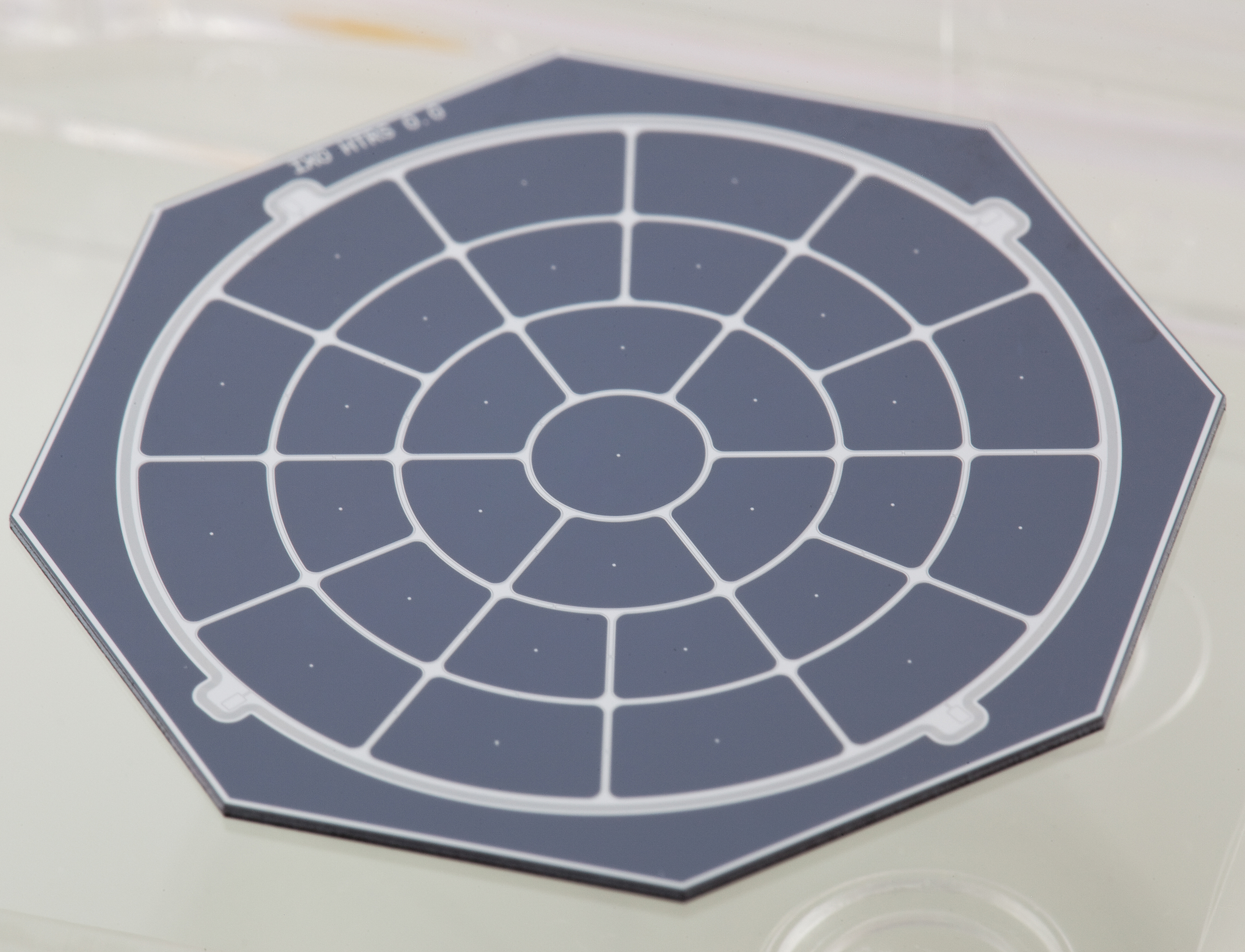
HTRS design on a dummy wafer, with the 31 SDDs clearly visible. The images show the entrance window and the back side of the array. Courtesy of Peter Lechner. Click the image for a larger view
The SDD is a completely depleted volume of silicon in which an arrangement of increasingly negatively biased rings drive the electrons generated by the impact of ionizing radiation towards a small readout node in the center of the device. The time needed for the electrons to drift is much less than 1μs.
The main advantage of SDDs over conventional PIN diodes is their small physical size and consequently the small capacitance of the anode, which translates to a capability to handle very high count rates simultaneously with good energy resolution. To take full advantage of the small capacitance, the first transistor of the amplifying electronics is integrated onto the detector chip. The stray capacitance of the interconnection between the detector and amplifier is thus minimized and, furthermore, the system becomes practically insensitive to mechanical vibrations and electronic pickup.
 Top
Top