nasa logo, link to nasa home page Goddard Space Flight Center
NASA
> GSFC > Astrophysics Science Division > IXO
   + Search NASA
+ Google Search IXO
+ Intranet + Fast Facts + FAQs + Contact Us + Site Map
This website is kept for archival purposes only and is no longer updated.
+ Home + Science + Technology + People + News + Resources

Silicon Pore Optics

Material

The Silicon Pore Optics approach uses commercial, high-quality 1mm thick silicon wafers as a base material. The latest generation silicon wafers have a surface roughness that is sufficiently low for X-ray reflection, are plane parallel to better than a micrometer, have almost perfect mechanical properties, and are considerably cheaper than other high-quality optical materials.

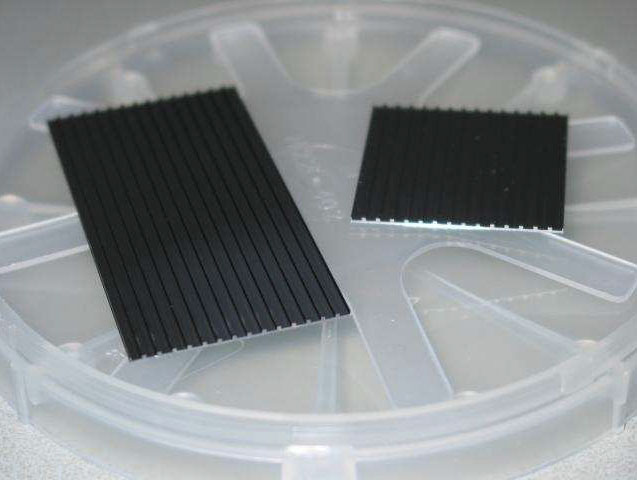
The optics are built up from rectangular cuts of commercial silicon wafers.

+ Larger Version

Figures are courtesy of Marco Beijersbergen et al.

The wafers are processed chemomechanically such that ribs remain, providing a thin membrane with ribs of very accurate height and highly polished surfaces.

+ Larger Version

top of page Top

Assembly

  1. The process starts by taking 6-cm-wide rectangular cuts of wafers and treating the backside with a chemo-mechanical process such that ribs remain with a very accurate height and a highly polished surface.
  2. One side of the segment is then structured via etching with accurately wedged ribs approximately 1 mm apart. The other side is coated with X-ray reflecting metallic layer.
  3. The ribbed plates are then stacked onto a cylindrical mandrel, forming a pore structure.
  4. To stack the plates, they are bent into a cylindrical shape with the required radius, and then pressed onto the previous plate. This results in a direct optical bond between the highly polished ribs and the surface of the previous plate.
  5. After the stack is built it can be raised in temperature to turn it (partially) into a true covalent bond. Two stacks are co-aligned into a module forming an approximation of a paraboloid-hyperboloid mirror. The radial ribs of the pore structure provide extreme stiffness and stability and therefore allow the walls to be thin. The accurate height of the ribs, a direct result of the good plan-parallelism of the wafers, ensures that the plates are accurately concentric cylindrical or conical surfaces.
  6. A total of 236 modules form a "petal"—an azimuthal segment of the full mirror.
  7. Eight such petals form the complete mirror.
  8. Hard X-ray sensitivity is provided by coating reflecting surfaces at the innermost radii with multi layers.

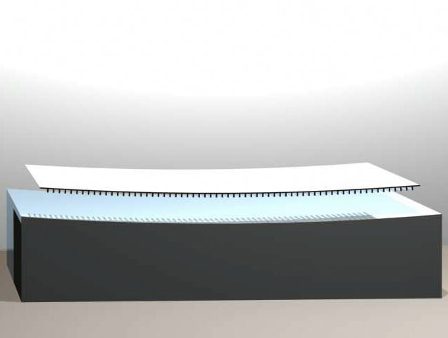
Ribbed plates are stacked onto a mandrel that provides the correct starting curvature.

+ Larger Version

Figures are courtesy of Marco Beijersbergen et al.

The ribbed plates are then formed a pore structure.

+ Larger Version

top of page Top

An automated optical assembly system was developed and placed in a class-100 clean room environment. The system is fully computer-controlled and has a number of actuators, some of them nano-actuators, an interferometer, digital microscopes with real time image analysis, and force sensors.

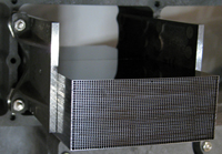
A 6cm wide Silicon Pore Optic module.

+ Larger Version

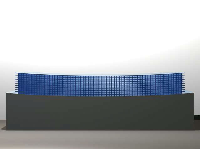
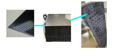
Silicon Pore Optic module assembly. Left - a ribbed silicon plate. Middle - a pair of silicon plate stacks aligned and mounted to form a mirror module. X-rays are focused after 2 reflections from the mirror like surfaces. Right - 2 mirror modules mounted in a 1m high optical bench petal, to form part of the X-ray aperture.

+ Larger Version

Back to FMA page back

top of page Top


Back to FMA page back

top of page Top


esa jaxa nasa logos esa home page jaxa home page nasa home page